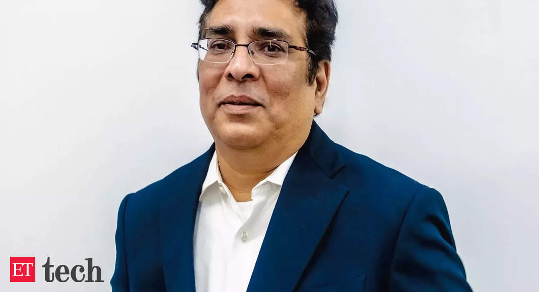
Samsung Semiconductor India Research has 1,100 patents: senior exec
“There are close to 4,000 engineers working from the Bengaluru R&D centre on some of the key technologies for Samsung semiconductors,” said Balajee Sowrirajan, corporate vice president and managing director of SSIR.
Talking about some of the product lines, he said, “some of the most advanced image sensors, of very high resolution, have been developed at SSIR and these are not just a first for Samsung, but are a first for the industry as well”.
For 20 years, SSIR has been entrenched into sensors, DRAM, storage solutions and neural processes. “We are world leaders in DRAM, or the volatile memories as we call them. We are a microcosm of Samsung Semiconductors in Korea. We work on all these areas,” Sowrirajan said.
Dynamic random access memory (DRAM) is a type of semiconductor memory that is typically used for the data or programme code needed by a computer processor to function. DRAM is a common type of random access memory (RAM) that is used in personal computers (PCs), workstations and servers.
High-end phones today have one terabyte of storage and cars or automobiles might have four terabytes of storage in the days to come, he said, adding that storage is becoming a big need from a data point of view.
Discover the stories of your interest

A phone has an average of four camera sensors… accelerated AI needs processors which are specifically designed for neural networks, and a general-purpose CPU might not solve the problem, he said, explaining the need for the company’s products.“Sensors are an example. But there are many areas where we do very advanced product development. A good testimony of some of the product development and innovation is the number of patents from SSIR. We have close to 1,100 patents from SSIR. That’s another metric to see the kind of innovation we have from here,” he said.
SSIR has also collaborated in the electrostatic discharge (ESV) domain with Bengaluru’s premier science research university, the Indian Institute of Science (IISc). It is working with professor Mayank Shrivastava who is an expert in nanoelectronics and ESD.
“The project is progressing well with a lot of activities. It’s a multi-year project for us to come up with some very innovative ESD structures and is making good progress from both ends,” Sowrirajan explained.
In its three-year collaboration, the institutes will come up with ESD structures, which will be put on test chips. Once the test chip is validated, the structure will be finalised.
“We just had a first test chip done from both our ends. One is doing the design, and another is putting it on silicon and then studying the silicon results,” he said.
SSIR works both in the mobile and the automotive segment. “We do the IP design, and the software for many of the neural processing units. That’s one thing we do which is going to the end customers from an AI point of view,” he said.
On the use of AI in day-to-day design processes, he said, with chip sizes becoming more complex, and the amount of data to handle becoming more, the turnaround time is going down.
“The resources we use are going down. So, from that point of view, we must really use AI techniques. For example, a debug might take six hours. Can this intelligence be transferred to some kind of AI tool and be solved within 15-20 minutes?” he asked.
On the challenges in the semiconductor space primarily from a research point of view, he said the design complexities are increasing significantly.
“People are now talking about something called as chiplets. If I must implement a system, I still can’t do it on a single chip. I would have to do across multi-chip solutions. Multiple chips must come together to form a solution. With the complexity of the applications increasing, this is going to be a very important technology for us to address and master,” he said.
For all the latest Technology News Click Here

