
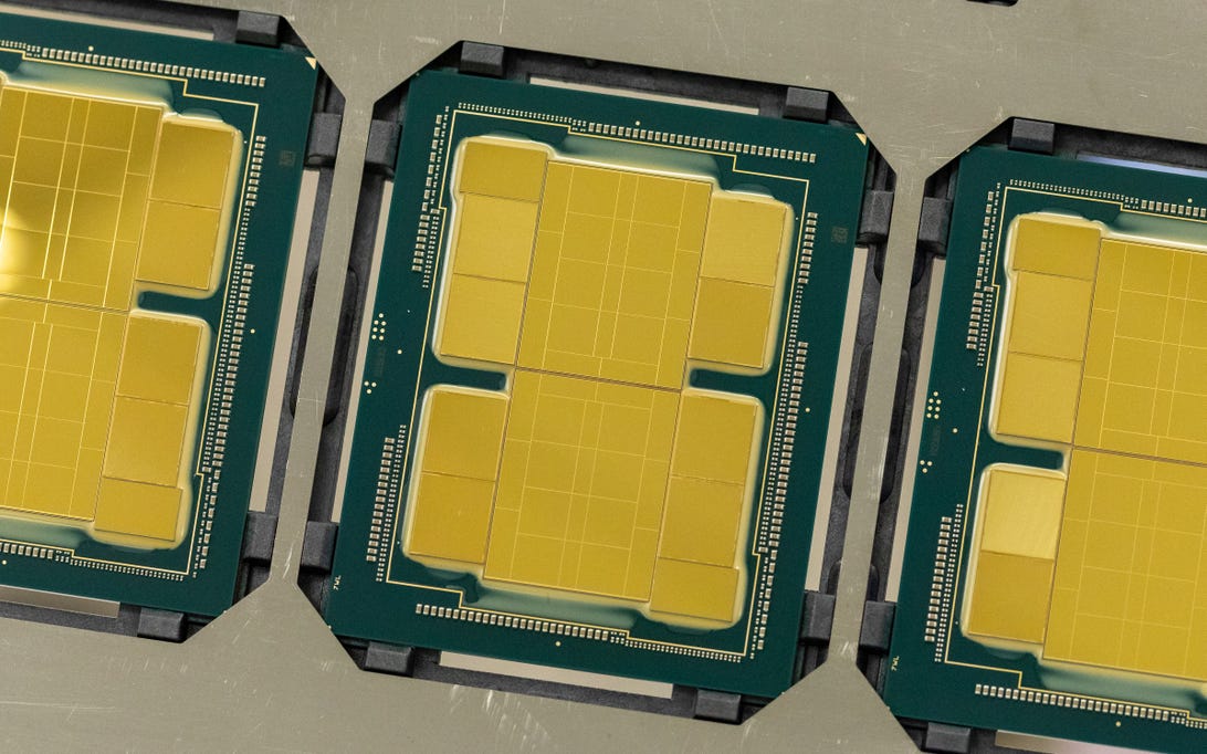
Intel packages several “chiplets” into one gargantuan Ponte Vecchio processor. The new UCIe alliance should make such packaging easier.
Stephen Shankland/CNET
Almost all of the world’s biggest chipmakers have banded together in an effort to make it easier to assemble processor elements called chiplets into one larger device. The effort stands to help keep Moore’s Law ticking, even as engineering difficulties and high costs hamper progress in semiconductor manufacturing.
Members of the new Universal Chiplet Interconnect Express (UCIe) alliance, announced Wednesday, include chip manufacturers Intel, Samsung and Taiwan Semiconductor Manufacturing Co. along with chip designers AMD, Arm, Google, Meta, Microsoft and Qualcomm.
Processors for years consisted of individual rectangles, complete chips packed with circuitry. Increasingly, though, chip designers and manufacturers are assembling collections of chiplets into larger devices. The idea, called heterogeneous integration, lets chipmakers reuse elements for years to lower costs, choose among manufacturers with different abilities and invest in the most advanced manufacturing only where it makes economic sense. That, in turn, should mean ever more transistors — chips’ core processing technology — for more advanced devices.
“We expect the UCIe consortium to foster a vibrant chiplet ecosystem,” Cheolmin Park, a vice president in Samsung Electronics’ memory business and one of several executives who praised, said the effort in a statement.
The most conspicuous absences from the list are Nvidia and Apple, neither of which commented for this story.
The most extreme example of this advanced packaging is Intel’s Ponte Vecchio processor, which combines separate chiplets for processing, graphics and memory into a mammoth device with more than 100 billion transistors. Ponte Vecchio’s number crunching and AI prowess is designed for the Aurora supercomputer, but packaging is spreading to more mainstream devices like new AMD processors employing the company’s 3D V-Cache memory packaging technology.
The UCIe effort is designed to standardize communication links among different chiplets, also called die since they’re diced from larger circular silicon wafers. Ideally, that should lower the barriers for all chip designers to employ the approach.
For all the latest world News Click Here